Seeed FusionPCB
プリント基板、電子工作などに関する技術、情報まとめのブログです。
つまりプリント基板穴は、部品接続・配線接続・固定などの目的で設計された重要な構造です。
もし「なぜ穴が必要なのか」や「ビアの仕組み」など詳しく知りたければ、そこも説明できます。
Your email address will not be published. Required fields are marked *
Comment
Name *
Email *
Website
Save my name, email, and website in this browser for the next time I comment.
Notify me via e-mail if anyone answers my comment.
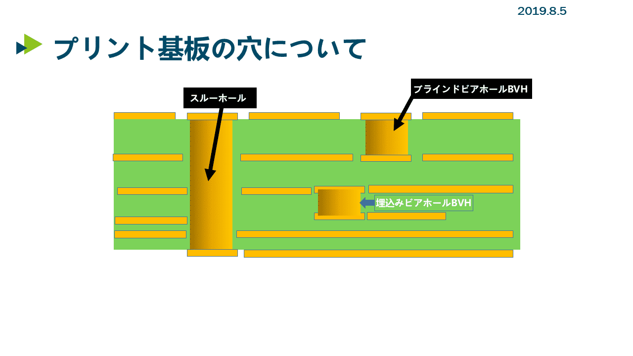

つまりプリント基板穴は、部品接続・配線接続・固定などの目的で設計された重要な構造です。
もし「なぜ穴が必要なのか」や「ビアの仕組み」など詳しく知りたければ、そこも説明できます。